The SEP protocol serves for communication between the MR25 or MR400 communication unit and the SEP technological measuring unit. It enables data to be transferred from 8 binary inputs with 8 counters, 8 binary outputs, 8 analog inputs and 2 analog outputs and.
A description of the SEP technological unit can be found in the: Products/Hardware/Accesories/SEP section on the Racom pages, www.racom.eu.
The structure of the SEP packet transmitted from the protocol to the MORSE network is given below:
| BO/8 | BI/8 | 8xAI/16 | temp/16 | 2xAO/16 | 8xcount/32 | crc/16 |
| BO | – binary output – 1 represent a triggered relay |
| BI | – binary input – 1 is level H, i.e. the terminal is not tied
to ground |
| AI | – analog inputs in order |
| temp | – analog. Temperature of the processor |
| AO | – analog outputs in order |
| count | – counters in order |
The SEP protocol uses the MODBUS industry standard in RTU mode when communicating with the SEP unit. The reference manual of this standard can be found at www.modicon.com and therefore its description is not included in this document. The protocol does not support the whole set of MODBUS functions; only functions for work with inputs/outputs and certain types of registers are implemented.
The format of modbus commands is also given in the article “Format of MODBUS frames for MORSE” (MODBUS – format).
| Area | Func | Type | Range of addr(hex) | Content | ||||||||||||||||||||
| Dout |
|
|
|
| ||||||||||||||||||||
| Dinp | 0x02 | R |
|
| ||||||||||||||||||||
| Ainp, Aout, Count |
|
|
|
| ||||||||||||||||||||
| Flash |
|
|
|
|
The 0x1E function, which simplifies communication
between SEP and the higher-level system, was added to the standard
functions. It simultaneously enables all SEP states to be read and the
necessary outputs to be set during one poll.
The higher-level processor takes on the role of the master device. The connected SEP is always the slave. This configuration is firmly fixed and cannot be altered. So, as the standard MODBUS commands, the master cyclically polls individual slaves and processes their responses.
For orientation purposes we show the structure of normal packets and the principle of CRC generation:
Query (from master):
|Adresa/8 |Funkce/8 |Start/16 |Number/16 |CRC/16 |
Response (from slave):
|Adresa/8 |Funkce/8 |Count/8 |Data/8x count |CRC/16 |
The CRC uses polynomial 0xA001. It can be generated from a table or by means of a cycle and bit rotation. Generation using a table is eight times faster than a calculation in a cycle because there is no need for rotation of each byte in bits.
0x01 – READ_OUTPUT_STATUS
This function serves for reading binary outputs. Address space for this function is as follows:
Start: 0x00 - 0x07, 0xF0Number:0x01
- 0x08 , at address 0xF0 1 is obligatory
These numbers represent the start address and number of required
elements. It should be emphasised that the address sum and number of
elements cannot exceed the highest possible address. Upon exceeding a
random value outside the permitted range an
EXCEPTION_RESPONSE is returned. This rule applies to all
functions without exception.
0x02 – READ_INPUT_STATUS
This function serves for reading binary inputs. Address space for this function is as follows:
Start: 0x00 - 0xFFNumber:0x01 -
0x08
0x03 – READ_HOLD_REGS
Memory registers are read with this function. Internal flash memory, in which constants for analog inputs/outputs are stored, is also mapped into these registers. Address space for this function is as follows:
Start: 0x00 - 0x07Number:0x01 -
0x08
0x04 – READ_INPUT_REGS
Analog inputs and counters are read with this function. Values
(except for counters), returned by this function, are converted to the
set range, i.e. the analog input range (e.g. 4– 20 mA) is converted to
the size of the physical variable. Limits for conversion are stored in
flash memory and they can be modified using program
conf.exe. Each input can be configured separately.
Counters can be set and reset. Address space for this function is as
follows:
Start: 0x00 - 0x08 – for analog
inputs 0x09 - 0x0A – for analog
outputs 0x10 - 0x20 – for counters
Counters are read as normal 16-bit registers although their actual capacity is 32-bit. This means that it is a good idea to read at least two registers at a time (from even addresses) so that the complete contents of a counter are obtained.
It should also be emphasised that these counters have an order of bytes which is more jumbled than usual. A normal 32-bit word is organised as follows:
| 0 | 1 | 2 | 3 |
| MSB | LSB |
Example 1. state of counter 00000124 in the SEP packet in the MORSE network:
08:28:22.401| |69112202 69112201|S00I OUT 58| 89 0user
FF7E 0391 00A4 032C 02D6 0317 033D 02E3 02EE 000E 0016 0000 0000 0124 0000
---- ----As MODBUS is bit-oriented and not word-oriented the order of bytes becomes jumbled in counters. This fact should be taken into consideration in the higher level system. The order of bytes in counters now looks as follows:
| 3 | 2 | 1 | 0 |
| LSB | MSB |
Example 2. state of counter 00000124 in Modbus frame on the RS485 link:
08:28:22.351 tx 8 | S00
0104 0010 0010 F003
08:28:22.396 rx;i 37 | S00
0104 2024 0100 0000 0000 0000 0000 0000 0000 0000 0000 0000 0000 0004 0000
-- ---- --0x05 – FORCE_SINGLE_OUT
This function serves for setting binary outputs. Address space for this function is as follows:
Start: 0x00 - 0x07
0x06 – FORCE_SINGLE_OUT
Memory registers can be modified with this function. Since internal flash memory is also mapped into these registers this memory needs to be unlocked by making an entry to a “special binary output“. The memory is automatically locked again after a successful entry or after 10 sec. This prevents unwanted overwriting of the constant in SEP during labouring or in the case of an unsuitably programmed master. In practice this means two acts:
Entry of log. 1 to the reserved address 0xF0 in binary outputs, the chip acknowledges this entry in the normal manner.
Entry of the value into flash memory. Memory is then automatically locked. Entry is again acknowledged in the normal manner.
f the flash memory is not unlocked beforehand SEP will still
acknowledge that the entry is correct but will not actually do anything.
The state of memory locking can also be read with a 0xF0
binary output status request. Log. 1 signifies it is
unlocked. It is not necessary to maintain the immediate order of
unlocking, entry, as it is possible to insert the order of other queries
between these two actions. It is only necessary to take automatic time
locking into account. When setting up counters it is necessary to be
aware that they are 32-bit counters and that the whole counter needs to
be written to – two consecutive entries or use function
0x10.
Address space for this function is as follows:
Start: 0x00 - 0xFF – for flash
0x100 - 0x101 – for analog outputs 0x110 -
0x130 – for counters
0x0F – FORCE_MULTIPLE_OUTS
This function can be used to advantage for setting up binary outputs. This function is able to set up all outputs according to the applied mask. Address space is as follows:
Start: 0x00 - 0x07, 0xF0Number:0x01
- 0x08, – at address 0xF0 1 is
obligatory
0x10 – RESET_MULTIPLE_REGS
This function serves for mass setting of memory registers. What applies to function 0x06 applies to this function. Address space is as follows:
Start: 0x00 - 0xFF – for flash
0x100 - 0x101 – for analog outputs 0x110 -
0x130 – for counters
Number:0x01
      - 0x08
This function is not yet fully supported. We recommend using multiple polling of function 0x06 (FORCE_SINGLE_REG) instead.
0x1E – READ_ALL
This new function was added to the protocol for easier overall control of SEP. The query/response pair enables the reading and setting of all inputs- outputs in one communication cycle. The form of queries and responses is somewhat different from the standard so a more detailed description is given below:
|Adresa/8 |Funkce/8 |Bin.Out/8 |An.Out1/16 |An.Out2/16 |Rez./8 |CRC/16 |
The states of binary and analog outputs are contained in a query, as is obvious. Binary states form an ordinary bit mask which is copied to SEP outputs after being correctly received. Analog values are first converted according to limits from flash memory and then set to the actual outputs.
|Addr/8|Funkce/8|Count/8|Bin.Out/8|Bin.In/8|An.In/9x16|An.Out/2x16|CRC/16|
Inputs and outputs in the response are up-to-date from the instant
of reading from SEP. The temperature of the AD converter chip is also
contained in analog inputs (input 0x08). Since this has a
negligible temperature rise this data can be taken as the ambient
temperature. This data is not converted because the unit is not designed
for measuring temperature – it is up to the higher-level system how this
value is handled.
SEP units can be arranged in different ways:
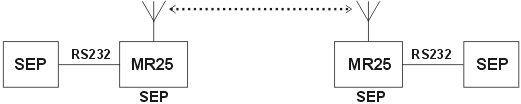
Connection of two SEPs via a radio link. States of inputs Dinp 0-7 and Ainp 0-1 are transferred to outputs Dout 0-7 and Aout 0-1 of the opposite station.
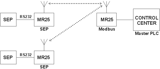
Connection of a greater number of SEPs to a control center. SEPs are Slaves and the states of their inputs Dinp 0-7 and Ainp 0-7 are transferred to the center. Outputs Dout 0-7 and Aout 0-1 are controlled from the centre.
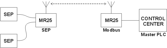
Connection of 1-3 SEPs over an RS 232 link to a common MR25 with control center. Functions as in example 2.
The SEP protocol uses the following functions for communication between the CU and SEP PLC:
04– for reading states of counters
1E– for writing and reading from binary and analog inputs and outputs
The resulting record of the state of the SEP is held in the CU memory. If this record is changed so that the different is greater than set limits a SEP packet containing the current state of the SEP is sent to the opposite station or to the center.
In the case of connecting two SEPs (fig. 1 above) this state is transferred to the opposite SEP.
In the case of the center (fig. 2) the SEP packet is stored in cache memory in the central CU, where it waits for a routine query from the Master PLC, which works in the Modbus protocol. Commands from the centre are sent as Modbus commands to the CU with the SEP protocol. They are transferred from here to the SEP PLC using functions
04and1E.
This function enables one SEP to communicate with several different opposite stations. Digital and analog inputs are divided into 8 groups:
Skupina:   obsahuje tyto kanály:
  No        Din  Dout  Ain  Aout
  0         0    0     0    0
  1         1    1     1    1
  2         2    2     2
  3         3    3     3
  4         4    4     4
  5         5    5     5
  6         6    6     6
  7         7    7     7
Each group has its own target address defined in the “(g)roup parameters” menu. These addresses can only differ in the last byte. Each group has its own opposite group assigned. Addresses and groups at both ends of the radio link must be defined reciprocally; see the configuration example.
The threshold “ani” for analog inputs and
“cnt” for counters are individually defined for each group.
Fields (t)hr and (c)thr in the SEP parameters
menu are not used in Group mode.
These are given in the separate article Protocol SEP for MORSE – examples.
A short example is given here only – the SEP packet and the Debug
message at the parameter “(D)ebug level:1“:
Monitoring: source 690F0002|5.
07:05:11.532  INPUTS CHANGED. SENT TO 690F0001
state: di 007F do 0002 anai0 0066 anai1 0057 anai2 0049 anai3 0057 anai4
005C anai5 0057 anai6 0049 anai7 0057 ao0 0000 ao1 000C
07:05:11.532|                 |690F0001 690F0002|S01I   OUT   58| 89 0user
027F 0066 0057 0049 0057 005C 0057 0049 0057 0045 0000 000C 0000 004C 0000
0004 0000 0000 0000 0000 0000 0000 0000 0000 0000 0019 0000 0000 8D66
The Debug message contains the state for Digital input, Digital output, Analog input, Analog output.
The SEP packet content:
02 | – digital output |
7F | – digital input |
0066 0057 0049 0057 005C 0057 0049 0057 – analog
input 0 to 7
0045 | – chip temperature |
0000 000C | – analog output 0 a 1 |
0000 004C 0000 0004 0000 0000 0000 0000 0000 0000 0000 0000
      0000 0019 0000
0000 | – counter states 0 až 7, counter state 0 is |
8D66 | – CRC |
SEP parameters:
p(a)rtner:690F0001h  t(i)me:60s  (p)oll:20*10 ms
net dead timeo(u)t:120s
analog (t)hr:250*10  (f)ilter:0
(c)ounter thr:2  (m)ask:FFh
init (d)igi outs value:0
i(n)it ana outs mode:all low value (0/4mA)
(N)egate digi outs mask:0h
(e)rr:SILENCE  (v)er:SEP 1.03 (old - before 11.2001)
(G)roup mode:OFF
(g)roup params
c(o)mpatibilty:OFF
for(M)at:SEP  (s)end counters:OFF
(A)out:4mA - 20mA  g(l)ue to resp:OFF
(D)ebug level:0

(T)est menu
(P)roduction
(o)ld menu (sw < 5.94)
(q)uit
>>
| Note | |
|---|---|
each parameter should be fulfilled, the value “???” must not remain |
| p(a)rtner:690F0001FFh |
| ||||||||||||
| t(i)me:60s |
| ||||||||||||
| (p)oll:20*10ms | = 200ms | ||||||||||||
| net dead timeo(u)t: 120s | No traffic timeout parameter. When timeout expires, outputs (digital and analog) are set to initial values according to (d) and (n). These initial values are are replaced with actual values. | ||||||||||||
| analog (t)hr:250*10 | = 2500 | ||||||||||||
| (f)ilter:3 | recomended values 1 (weak filtration) to 10 (strong
filtration) filter (low-pass filter) for limiting interference by
quick changes on the analog inputs | ||||||||||||
| (c)ounter thr:1 | sensitivity threshold of counters for causing transfer to the
center, number of pulses | ||||||||||||
| (m)ask:FFh | binary inputs, whose changes should be transferred are marked
with a bit mask | ||||||||||||
| init (d)igi outs value:0 | The default values of digital outputs. They are also used by communication failure, see “net dead timeo(u)t:”. | ||||||||||||
| i(n)it ana outs mode:all low value (0/4mA) | The values of analog outputs after launch and after failure
of communication. Optional: | ||||||||||||
| (N)egate digi outs mask:0h | Digital outputs are negated according to the selected mask. | ||||||||||||
| (e)rr:SILENCE | type of error message for a failure of SEP and higher-level system query:
| ||||||||||||
| (v)er:SEP 1.03 | Select the firmware version of the connected SEP.
| ||||||||||||
| (G)roup mode:OFF | Volba režimu Group
| ||||||||||||
| (g)roup params | Group processing: (c)enter:OFF local threshold | remote group tai cnt | address group ------------------+--------------- (0) 100 010 | 05h 1 (1) 050 001 | 06h 0 (2) 000 000 | 00h 0 (3) 000 000 | 00h 0 (4) 000 000 | 00h 0 (5) 000 000 | 00h 0 (6) 000 000 | 00h 0 (7) 000 000 | 00h 0 (q)uit >>
| ||||||||||||
| c(o)mpatibility:OFF |
| ||||||||||||
| for(M)at:SEP |
| ||||||||||||
| (s)end counters:OFF | – for MTF only
| ||||||||||||
| (A)out:4mA – 20mA | Analog input and output range (Only in MTF mode) | ||||||||||||
| g(l)ue to resp:OFF | glue content of cache to transparent responses | ||||||||||||
| (D)ebug level:1 |
| ||||||||||||
| (T)est menu | – Used for test purposes Test: Bin(O)ut (A)n out (G)et values (C)ounters (q)uit >>
|
| (P)roduction | – only for servicing purposes |